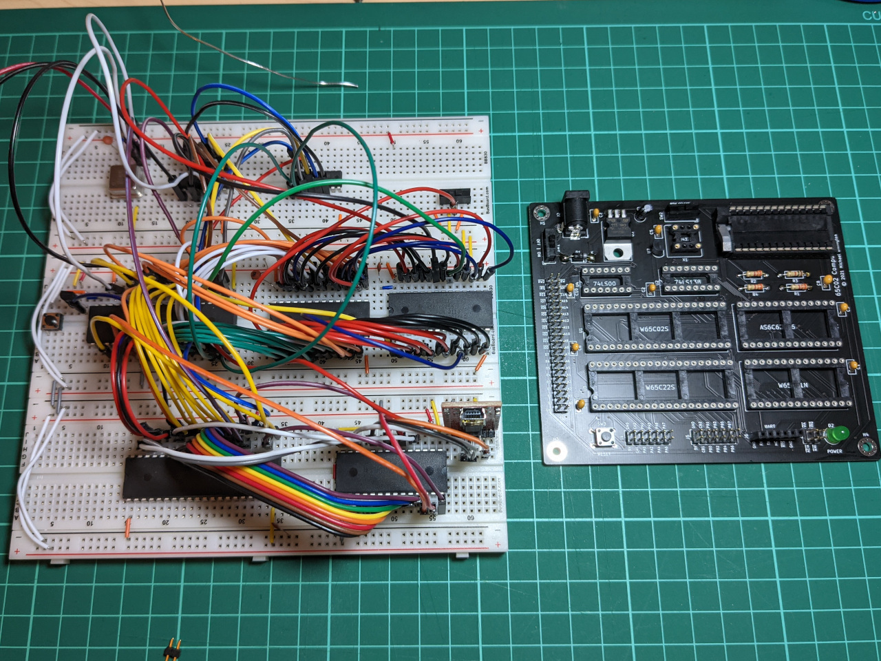
I’ve recently been working on building a 6502-based computer on breadboards as a learning project. After making a few revisions, and porting some software to run on it, I was confident that my computer worked well enough to connect up permanently on a circuit board.
This blog post about the process that I went through to convert my working breadboard prototype to a PCB. As somebody who is not trained in electronics, this involved some fresh challenges for me.
Schematic capture
As a first step, I needed to draw up a proper schematic in a CAD tool. I’ve already been learning to use KiCad’s Eeschema for schematic capture, so I went ahead and drew up the whole thing.
I decided to put all of the components on one crowded page, just because I haven’t learned to manage multiple pages yet.

Mostly, this was just replicating what I’d already built, but I also needed to:
- create a symbol for the DS-1813, which I could not find in the libraries I’m using
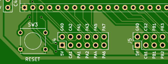
- decide on a pinout for expansion ports
- add a jumper block, so that the two interrupt lines (NMI and IRQ) can be disconnected from the on-board chips
I avoided changing the scope of the board to include important features (storage, audio), and instead added a header with all of the important buses and signals. My goal is to have a stable base system to work with, and I can always do a second board once I’ve figured out how these should work.
I did not use KiCad’s inbuilt BOM plugins, but instead manually wrote a parts list for future reference. The only components which I needed to order were sockets and pin headers, everything else was being lifted from the prototype.
Footprint assignment
Once the Eeschema electrical rules check was passing, I moved on to selecting footprints for everything. I spent quite a bit of time checking the datasheets for my planned components against the KiCad library to choose footprints that would fit.
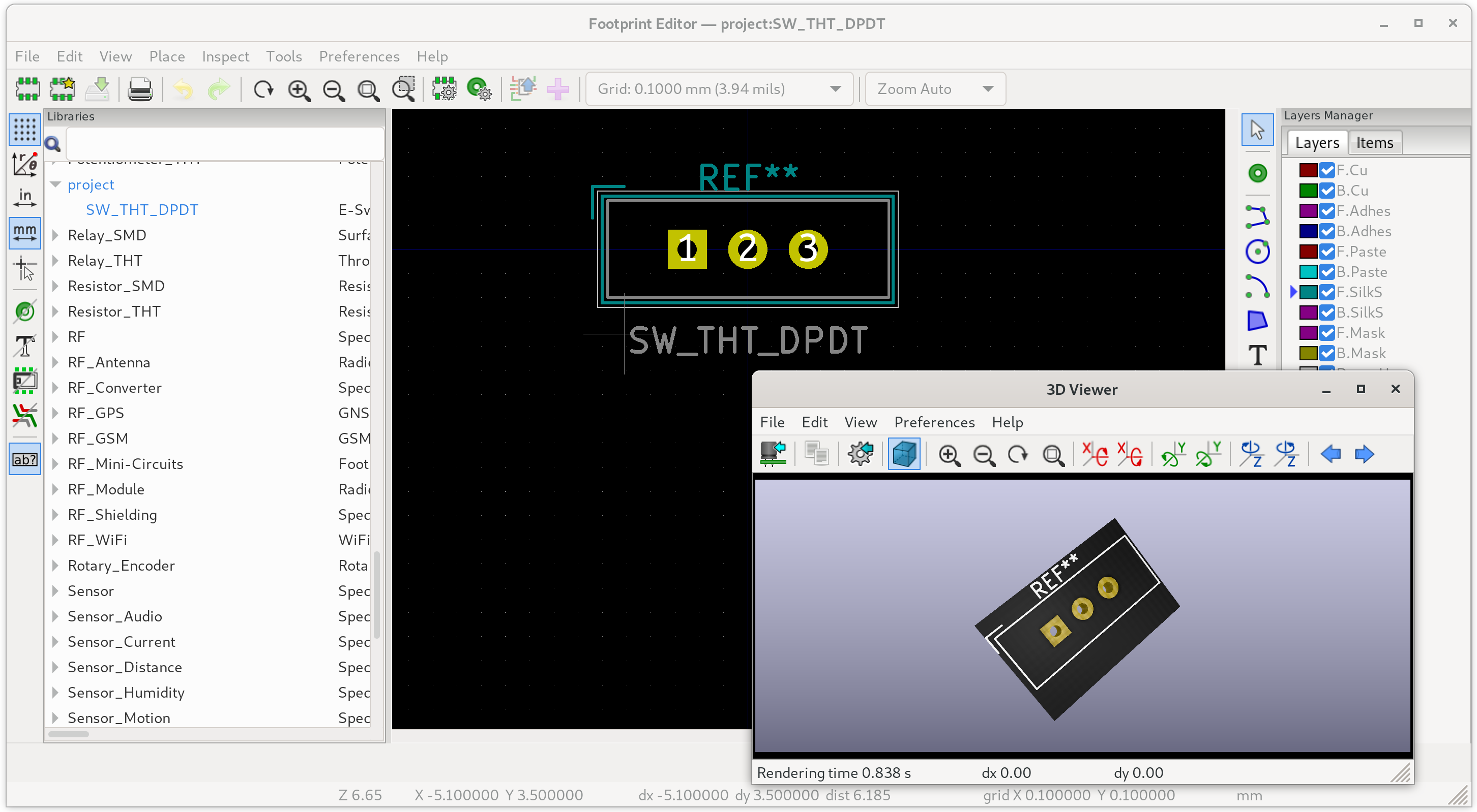
I could not find anything which matched the footprint of the mini SPDT switches that I’m using, so I made my own.
I had not yet chosen a ZIF socket for the EEPROM, so I selected a footprint for a standard socket instead. This was a risky move, because I had to guess how much space to leave when laying out the board.
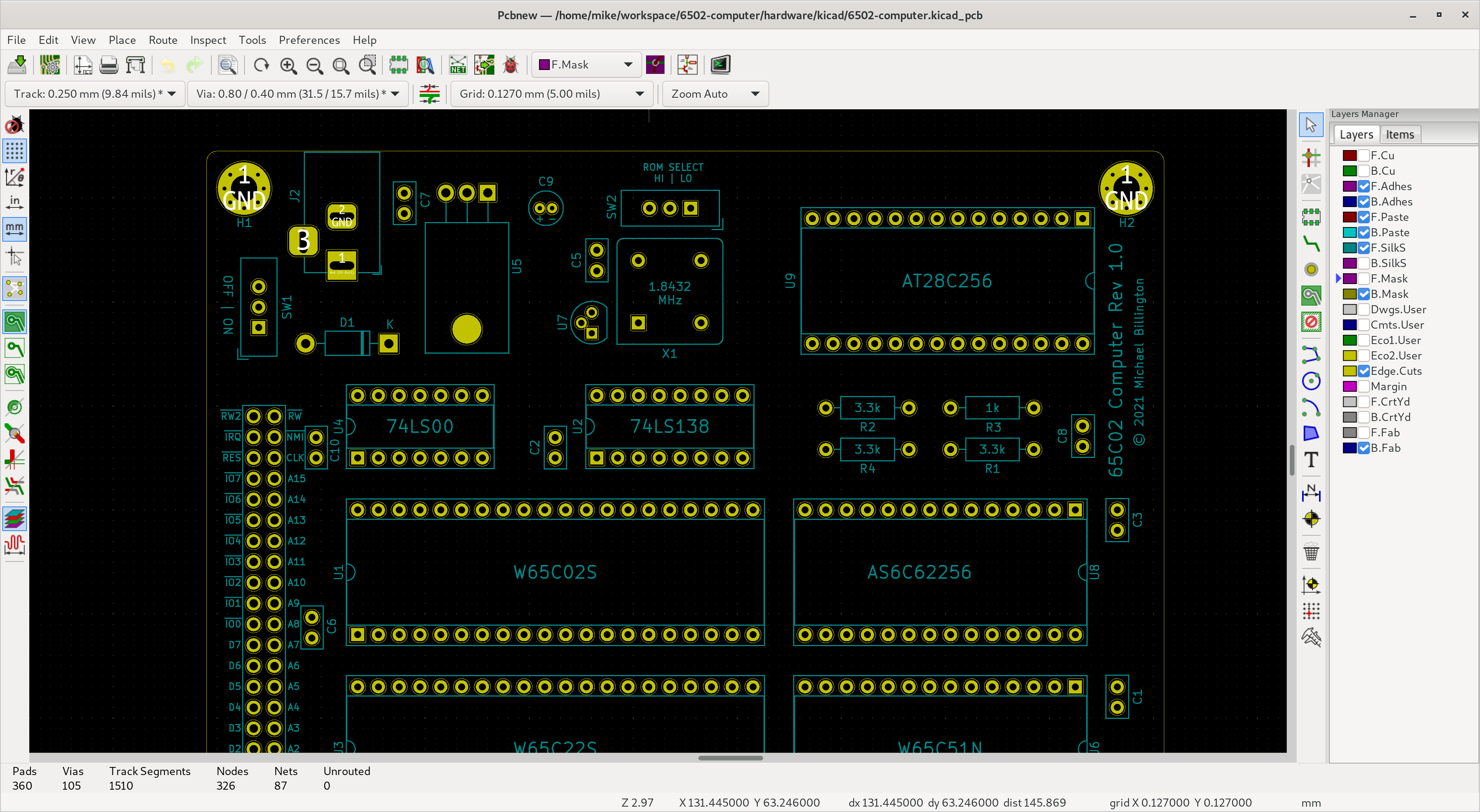
PCB design
I had already selected a board manufacturer, so I set up my track widths and via sizes according to their capabilities.
Next, I imported the netlist and placed the components. I attempted to fit everything in 10cm x 10cm, 2-layer board to save on manufacturing costs, but it was very crowded. I was worried about having enough space for traces, fitting an (unmeasured) ZIF socket, and adding some mounting holes, so I spaced it out to fit on a 10cm x 11.6cm board instead.
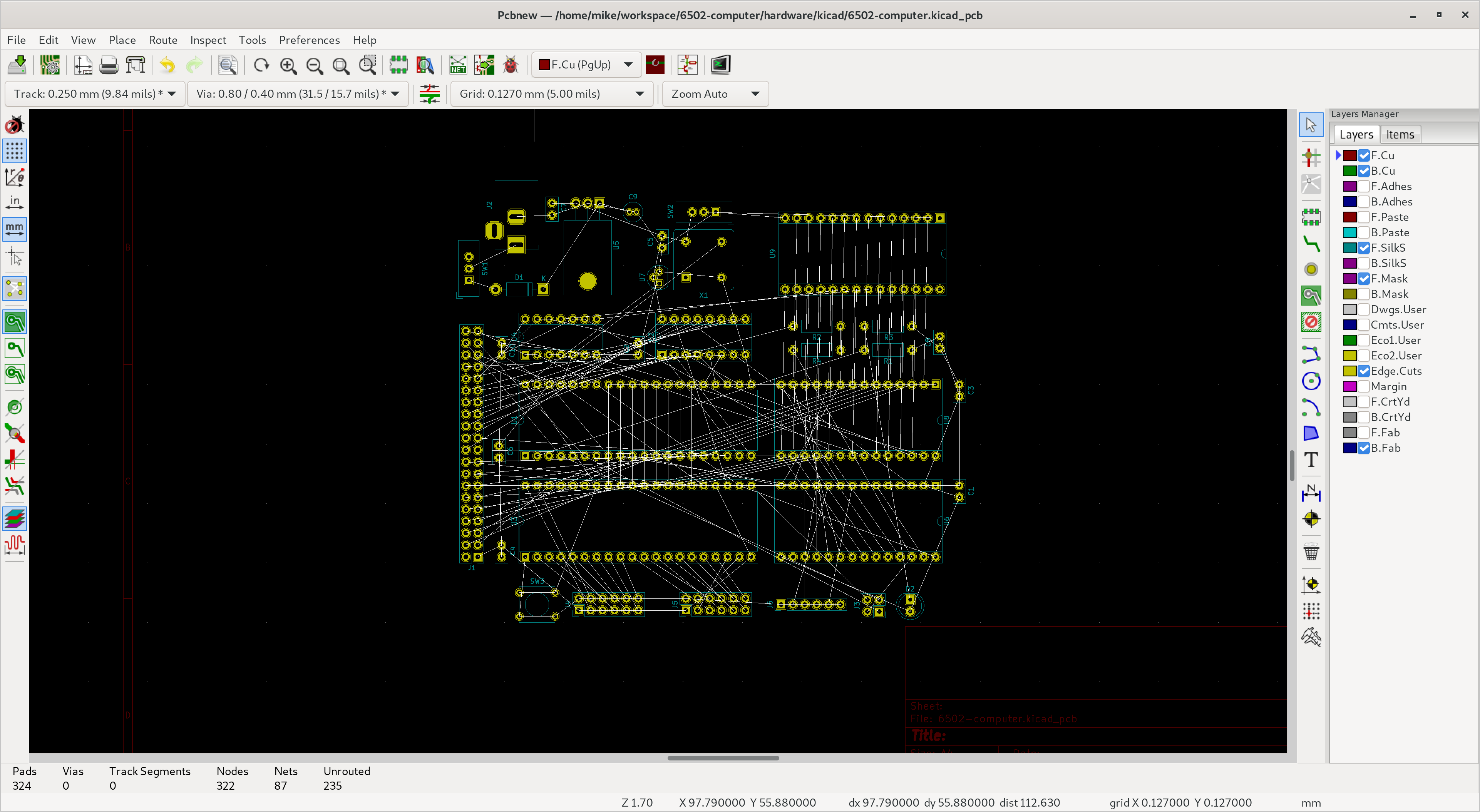
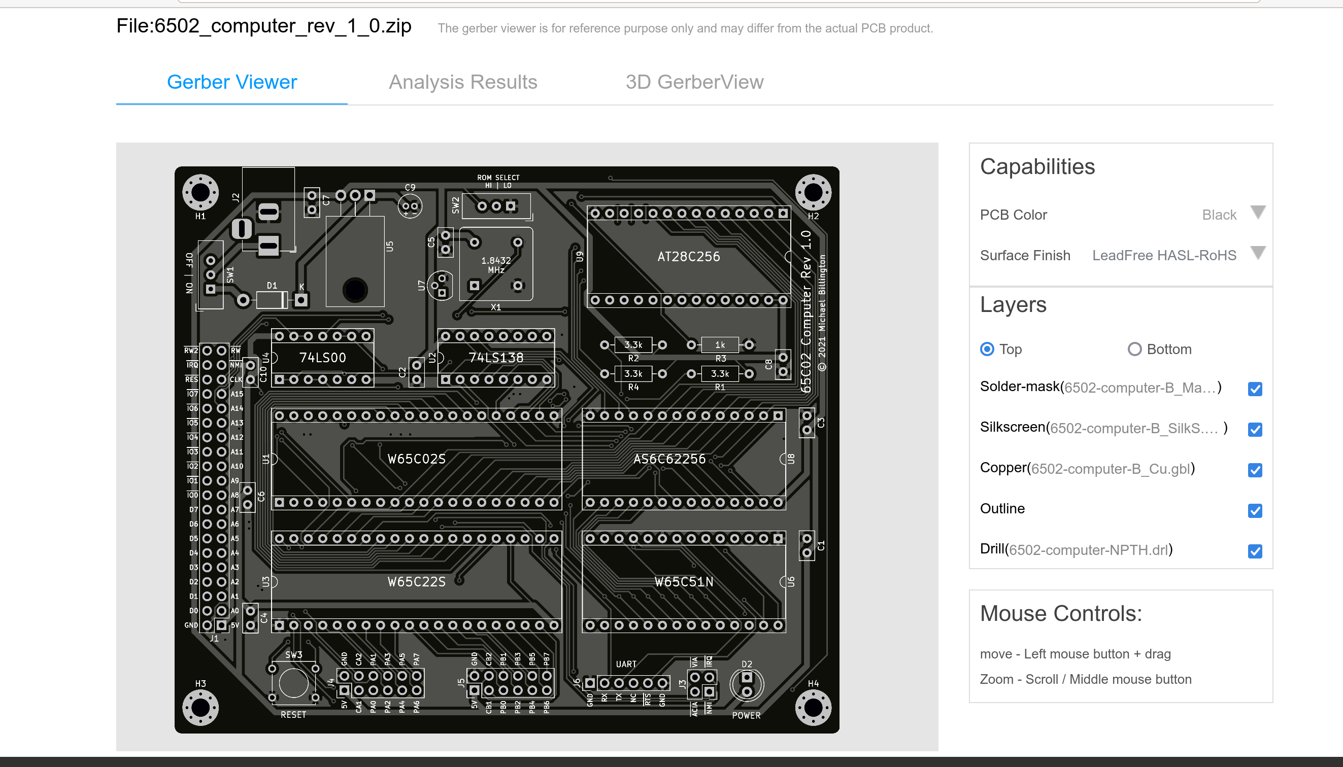
I also added footprints for M3-sized mounting holes, and edge cuts with rounded corners.
It took me 4 attempts to successfully route all of the traces. The result breaks every PCB layout best practice which I had read about, but I was happy just to have everything connected by that point.
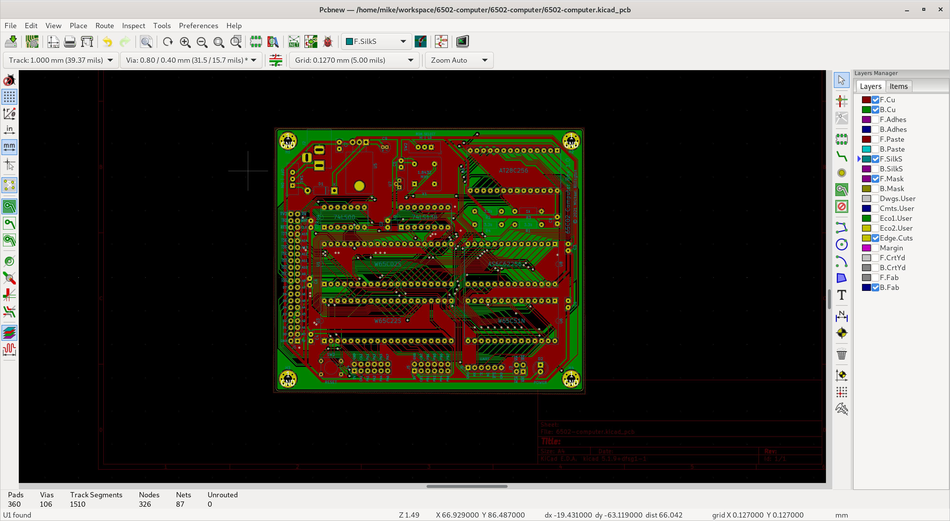
In hindsight, I could have made this task easier by splitting up the expansion header, and building an accurate footprint for a ZIF socket. I also could have placed the decoupling capacitors closer to the IC power pins, and avoided interrupting the ground plane.
The silkscreen setup was more time-consuming than expected. I wanted to make the board as self-documenting as possible, so that I would not need to open the design files on a computer when writing code and adding hardware peripherals. I labelled every switch, button, light and IC, as well as every expansion header pin (74 of them!). I also added some simple assembly hints such as resistor values, and +/- signs to indicate the polarity of the lone electrolytic capacitor.
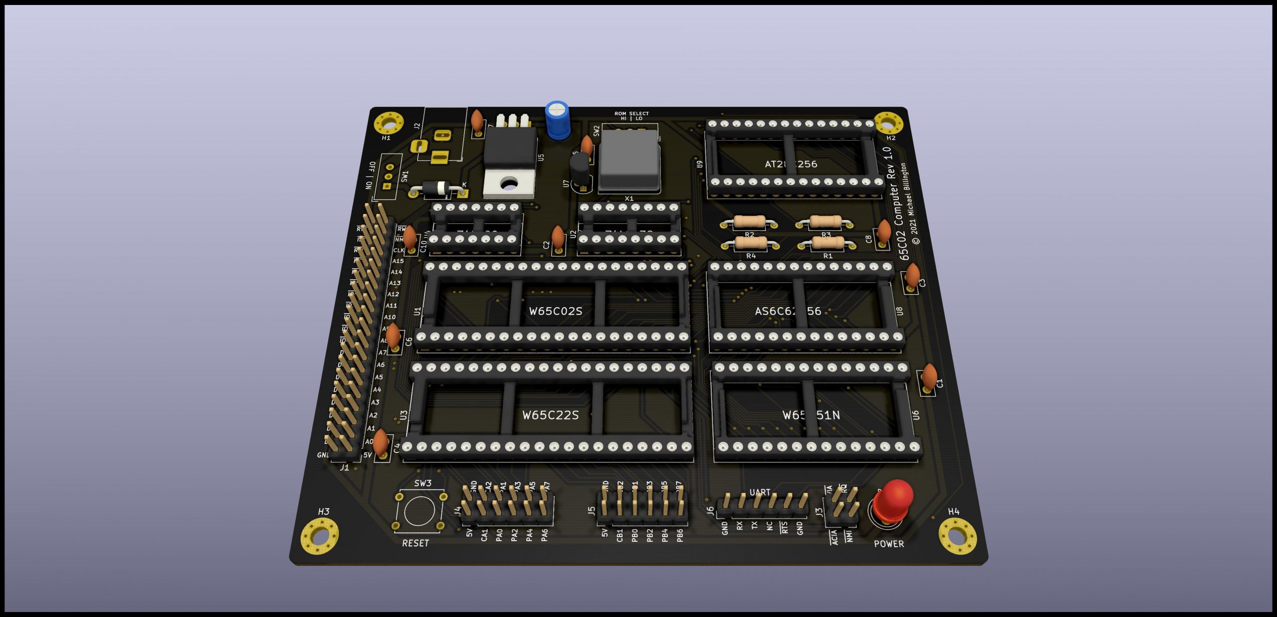
The 3D render view in KiCad shows how the finished board would look.
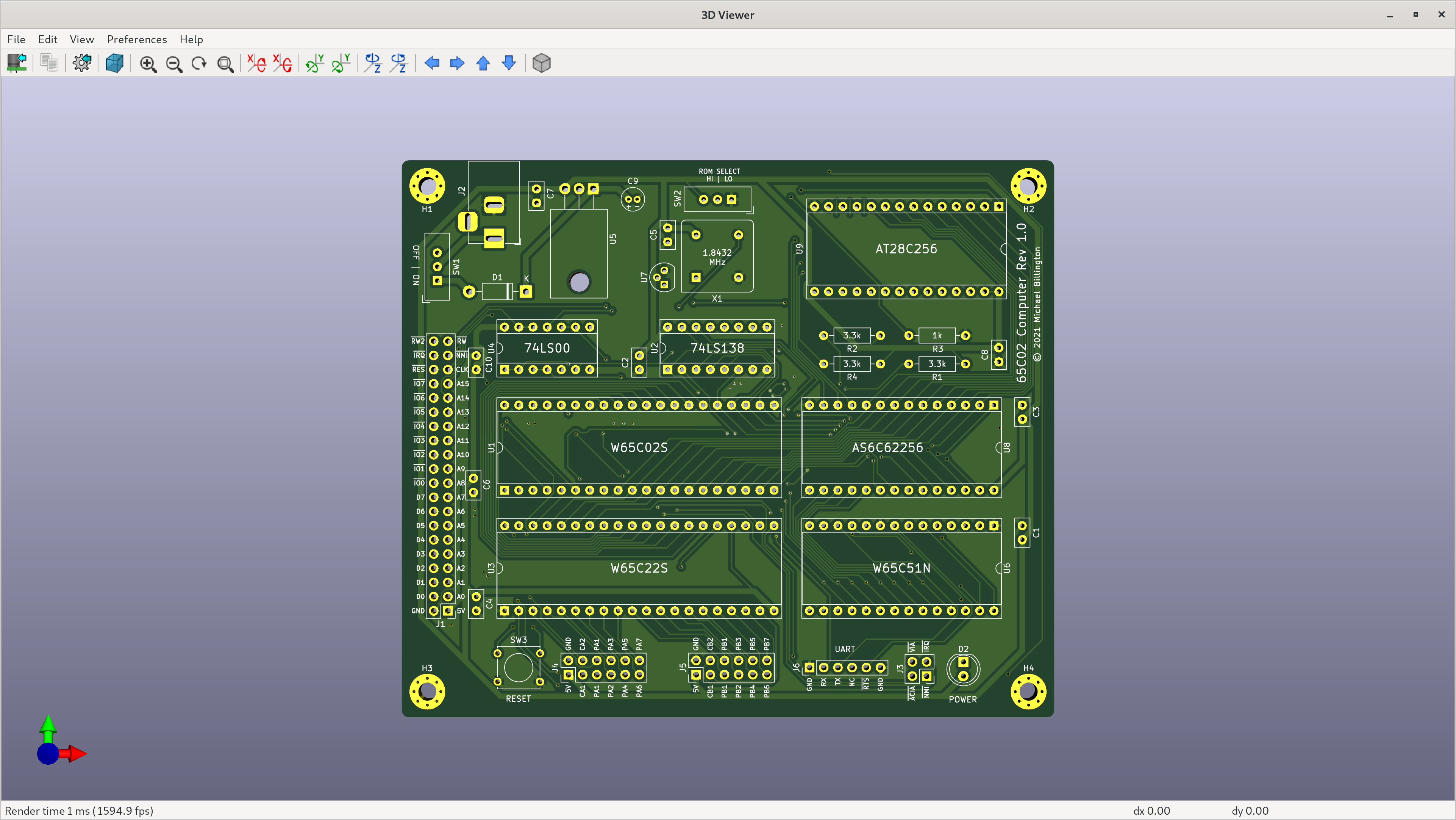
Components did not display on the board at first, but there is a menu option to download the 3D models. After setting this up, and setting the solder mask colour to black, I was able to render the board properly. This looks very similar to the assembled board, with just a few parts missing.
Manufacturing
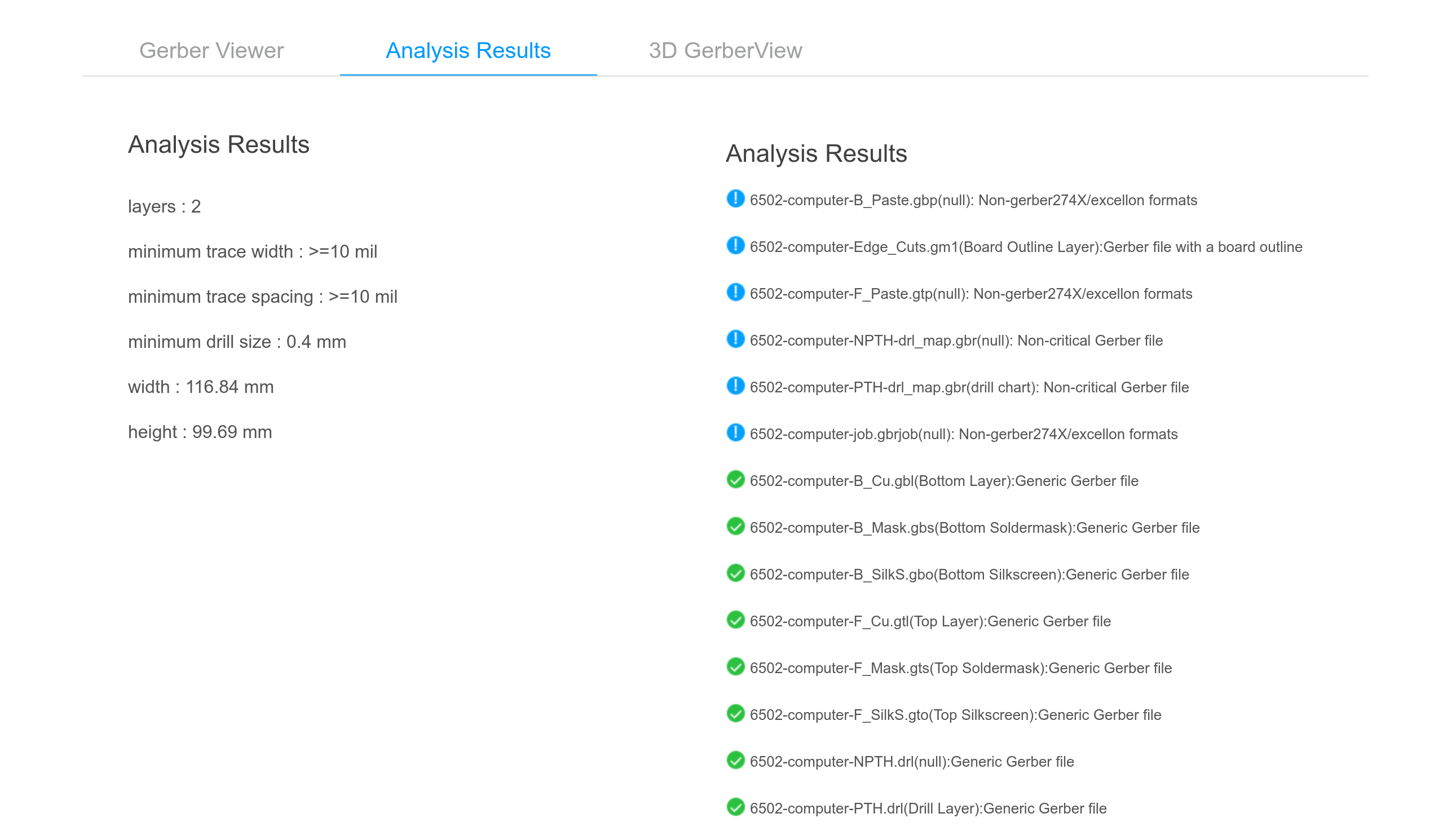
I only recently discovered that low-volume PCB manufacturing is accessible to hobbyists. Ordering the boards was really easy. I exported gerber and drill files according to their instructions, loaded them into a zip file, and uploaded them to a web portal.
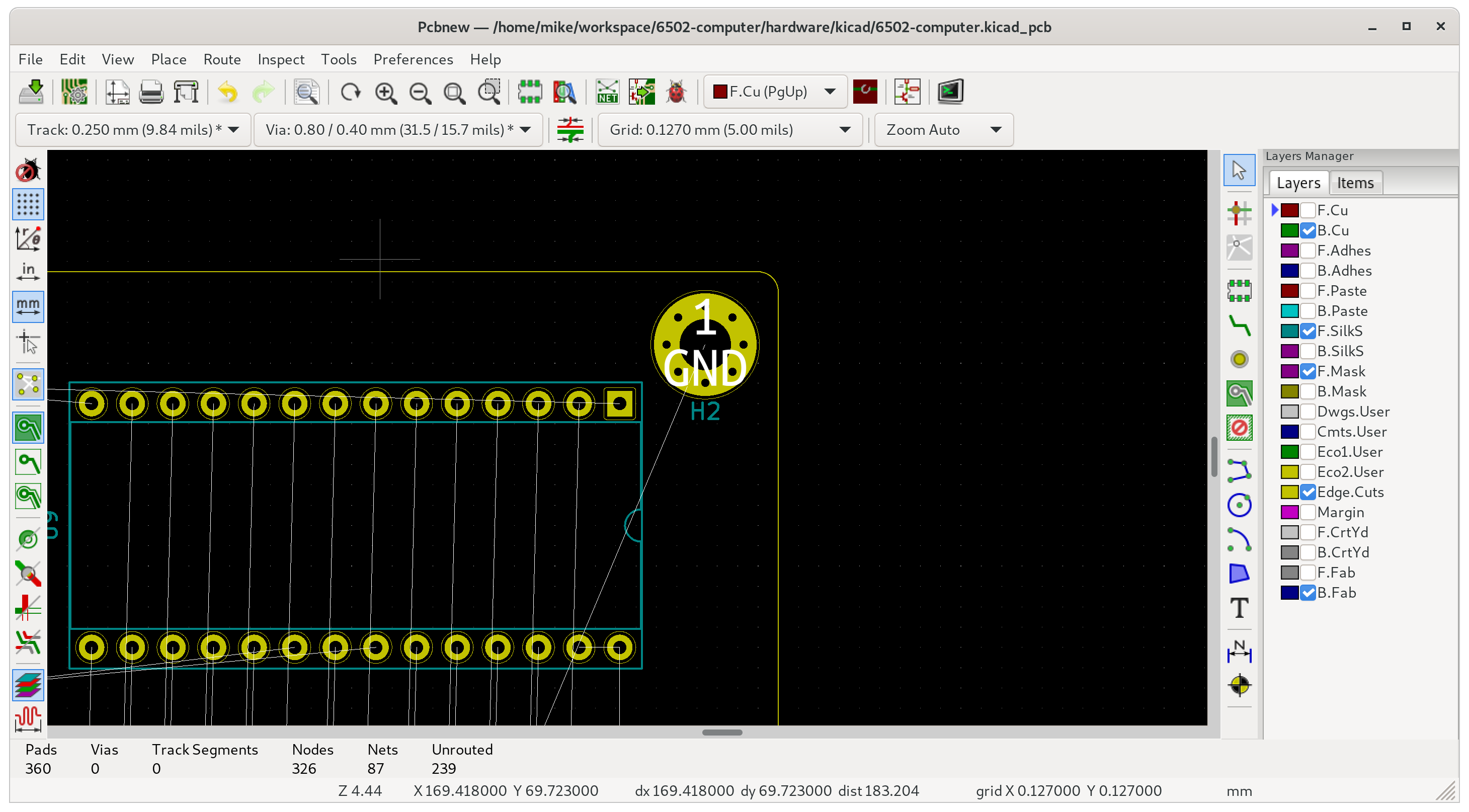
I am glad that an online gerber viewer was available, because it allowed me to spot an error which I had not noticed in KiCad, where I had two pins labelled PA1.
The default settings are reasonable, but I chose black solder mask, a lead-free surface finish, and chose the option to exclude the manufacturer’s order number from the board.
The gerber viewer also has a tab which shows checks against their manufacturing rules.
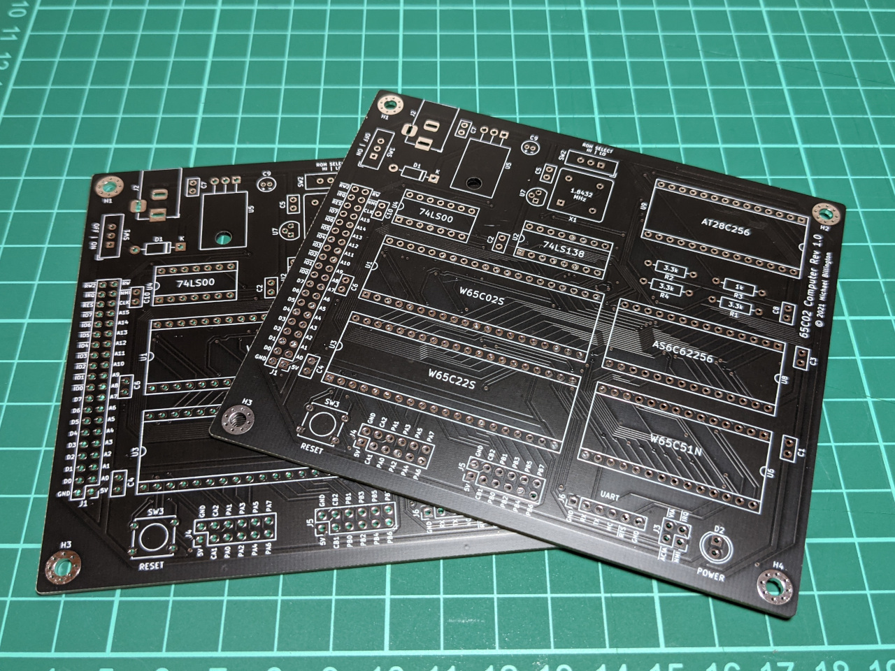
I placed the order, and eagerly checked each day as the boards progressed through the manufacturing steps. From placing the order to getting the boards on my desk, the whole process took 7 days.
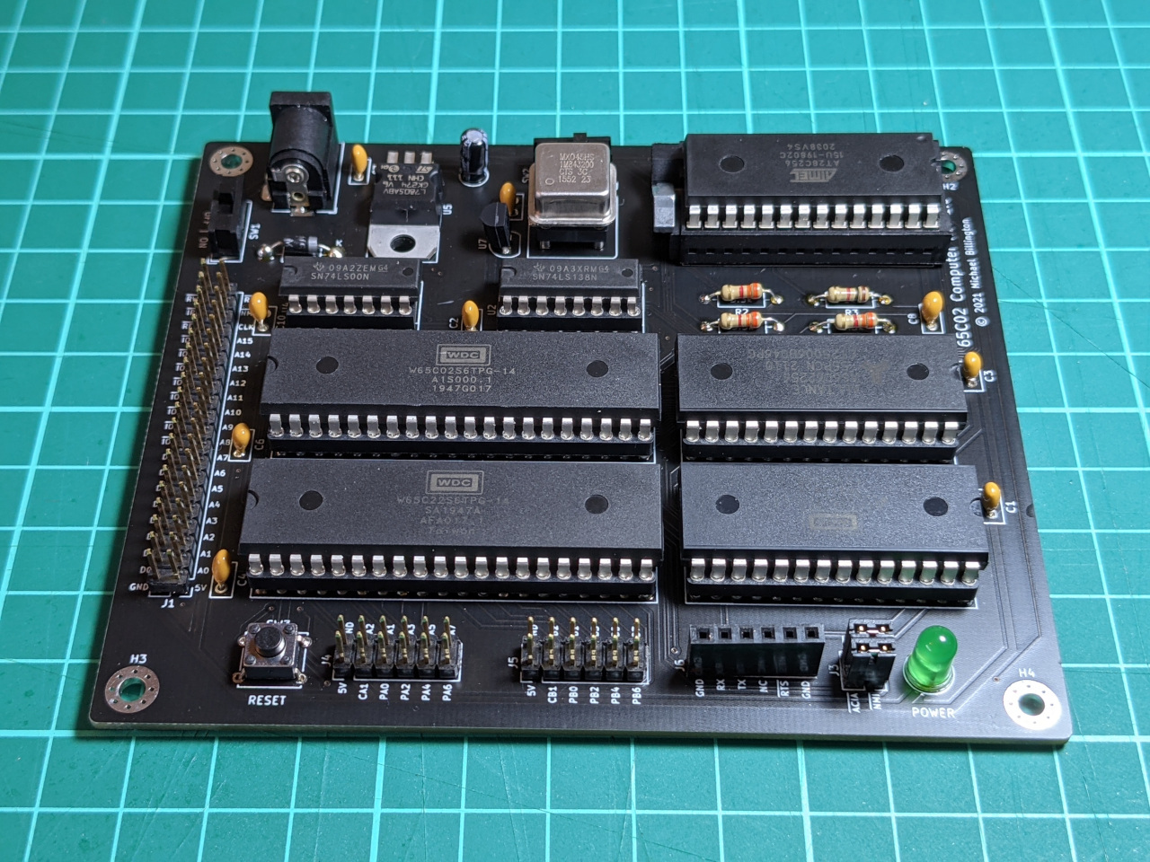
Assembly & test
Once all of the sockets arrived in the mail, I started assembling.
The standard advice I’ve read for through-hole assembly is to solder low-profile components first. Instead, I added enough components to light up the power LED.
I know that the power LED dims if anything is drawing too much current (eg. a short circuit). By getting this working first, I will know I’ve made a mistake (and can switch off the board quickly) if it doesn’t light up later.
I don’t think I’ve ever soldered more than a few pins or wires at a time, and this board had 323 pins to solder.
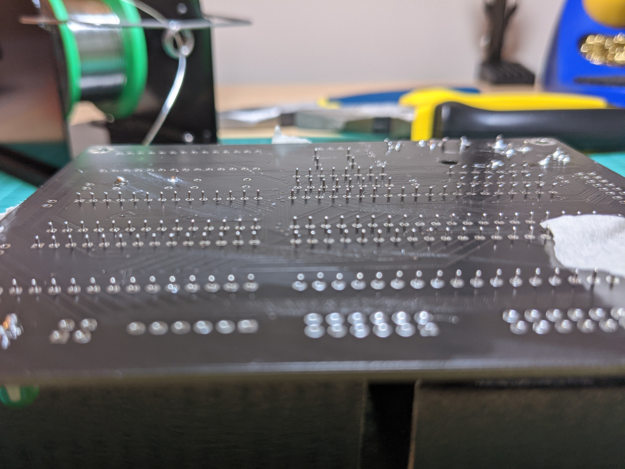
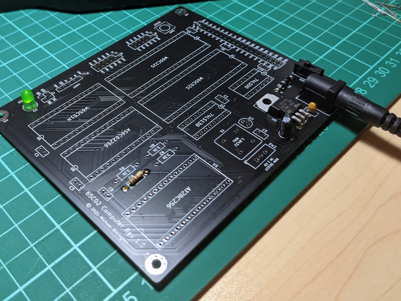
After a about 2 hours, I had a fully-populated board. It’s smaller and looks better than the breadboards, but it was time to move all the chips across to see if it actually worked.
Much to my surprise, the computer booted up to EhBASIC on the first attempt.
Wrap-up
This has been quite a fun project. It has proven to me that open source tools are perfectly sufficient for this type of hardware development. I’m also very happy to have reached a point where can call this project “done”, since I have a permanent home-built computer.
My plans for learning about low-level computing are not done yet, of course. I’ve kept everything at a low 1.8 MHz, so that I can continue to prototype hardware peripherals on a breadboard. I’ve also left a switch to select which half of ROM to boot from, so that I don’t brick my computer every time I make an error in an assembly language program.
I’ve uploaded the full parts list, design files, and firmware to GitHub at mike42/6502-computer.