In the last few months, I’ve been learning about the 65C816 processor, and trying to build a working computer which uses it. My latest breadboard-based prototype was not reliable, and I decided to convert it to a PCB to hopefully eliminate the problem, or to at least identify it.
Quick goals
I was aiming to make a debug-friendly 4-layer PCB, the size of two standard breadboards. This will be my first time designing a 4-layer board, and also my first time using KiCad 6 to create a PCB.
I didn’t have a working prototype, so I built in test points for connecting an oscilloscope or logic analyser to troubleshoot. In case of errors, I made it possible to leave some components unpopulated, and instead drive signals externally.
I also left some extra footprints which I might use for future improvements, or can fall back to if some of my ideas don’t work out.
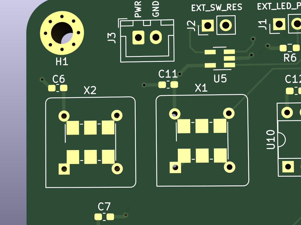
The clock
Some components require the inverse of the CPU clock, and there was previously a small delay from inverting the signal. I don’t think this is a problem on its own, but I introduced a D-type flip-flop to create a proper two-phase clock.
This does halve the CPU clock speed, so I added jumpers to allow an alternative clock source to be selected for the CPU, where previously the UART and CPU clocks needed to be the same. Note that there is an error in the wiring here, which I only discovered later.

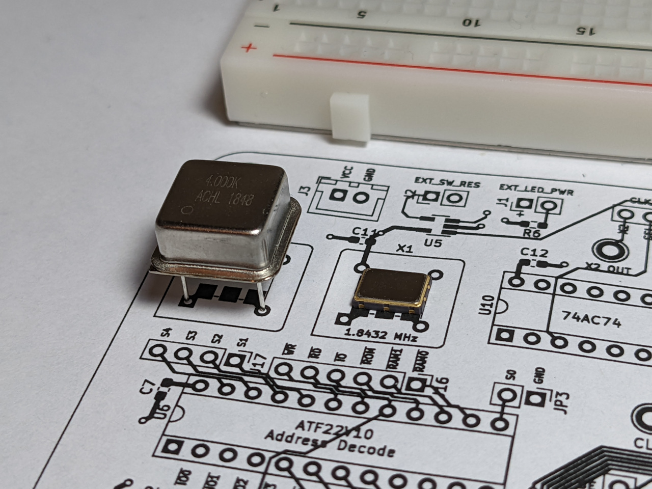
The oscillator I’m using on the breadboard prototype is a DIP-8 package. A larger variety of oscillators are available as a 5x7mm QFN package, where the four corner pins have the same function as the DIP-8 version. I added an alternative footprint, which fits without taking up any extra board space. I expect that I’ll only use this if I attempt to run the board at 3.3V later.
Some 6-pin QFN oscillators provide an inverted clock output on one of the pins, and it would be an idea to use one of those in a future design to reduce the component count.
New reset controller
Several components on the board require a reset input. These are mostly active-low inputs, but one component has an active-high reset. I discovered the tiny MIC2775 supervisory IC, which provides both.

I haven’t used this part before, so in case of problems, I also made it possible to remove this part and use a DS1813, which generates an active-low reset on my prototype.

These parts work by sensing voltage, and drop-in alternatives exist for either part if I move to 3.3V.
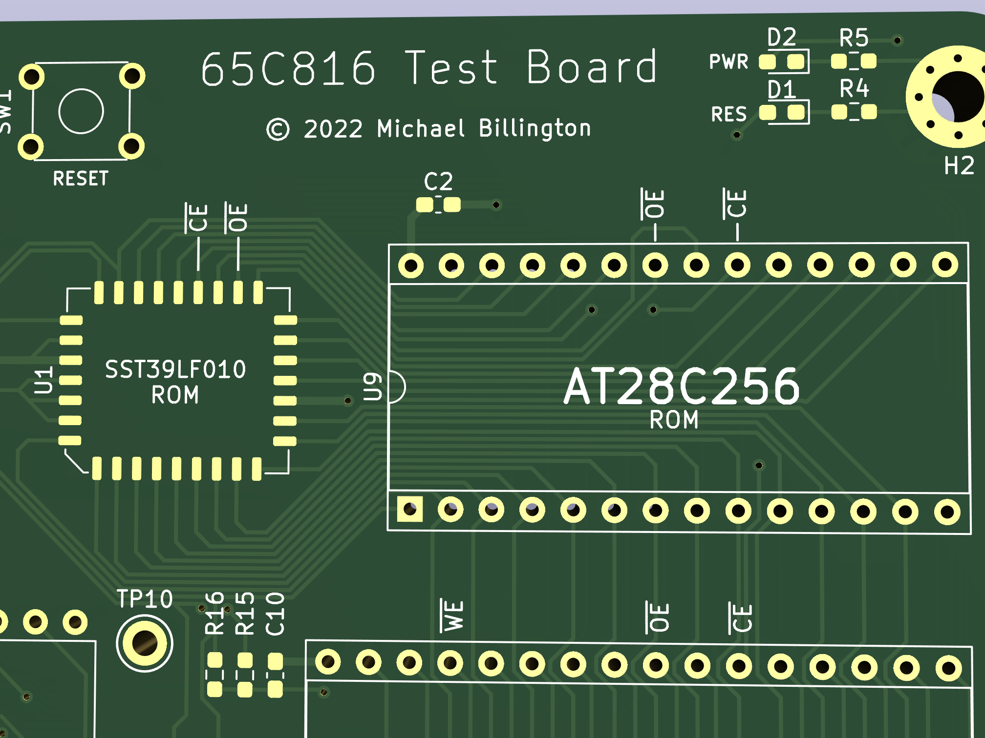
ROM
I am currently using a parallel EEPROM to store code for my prototype, and will add this to the PCB for this test board. As with the the clock and reset controller, I’m working with 5V components today, but considering what I would need to change to run the whole board at 3.3V.
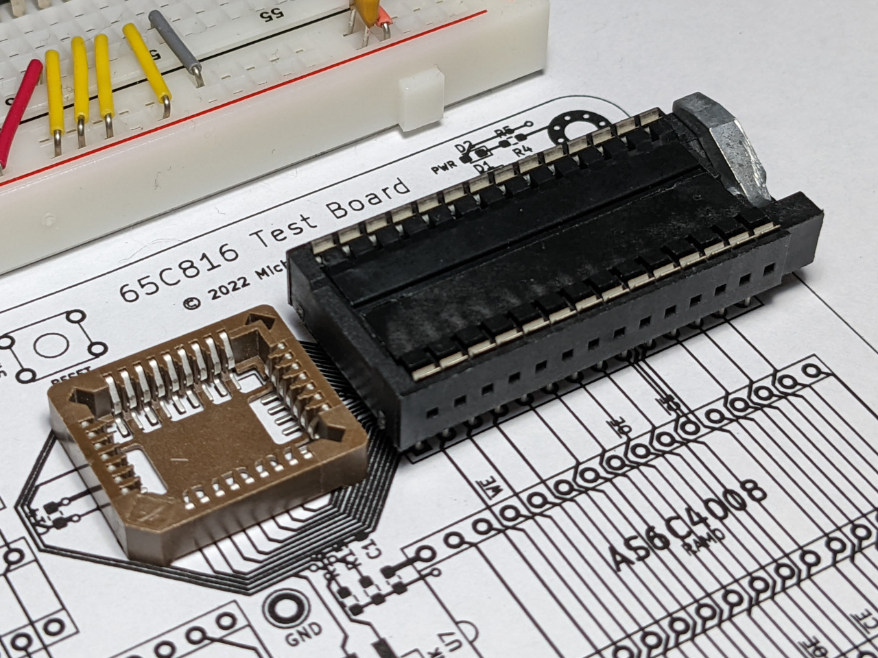
The few EEPROMs which are available at 3.3V use a different package, and are quite slow (200ns or worse). Parallel flash chips seem to be the most promising alternative, since they have a similar interface, although I haven’t confirmed that I can program them yet. I added a footprint for the SST39LF010, which also has a 5V variant with the same pin-out.
Other footprints
I also added footprints so that I could connect the SD card module which I used on my 6502 computer, a piezo buzzer, and some electrolytic capacitors if needed.
Design lessons learned
Although my first attempt at making a PCB was a success, I learned a few things which I’m using here.
For that previous project, I found that machined-pin sockets are not very tolerant of used chips with bent legs, so I’ve used cheaper stamped pin sockets for this test board. I’ve also left spacing at the ends of each socketed IC, so that they can be pulled out more easily.
I made an effort to keep unrelated traces away from points which I need to solder, because I had some problems with this on my last board.
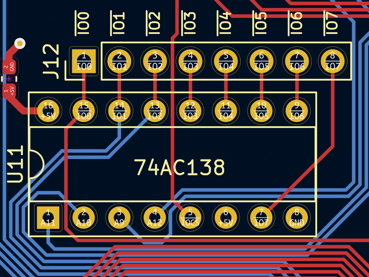
I also avoided creating one large expansion header, and instead exposed signals in places which are easy to route. For example, the I/O device select signals are exposed on a pin header right beside the chip which generates them.
PCB layout
The standard process is to make a schematic, then place components, then route traces.
For this test board, I instead chose the physical dimensions of the board first, and added components incrementally (particularly test points, expansion headers and alternative footprints) until I was making good use of the available space. KiCad has an item in the “Tools” menu to “Update PCB from Schematic”, which I used extensively.
Just to see how it would look, I also added the letters “65C816” to the back copper layer, which is visible in the top-right here.
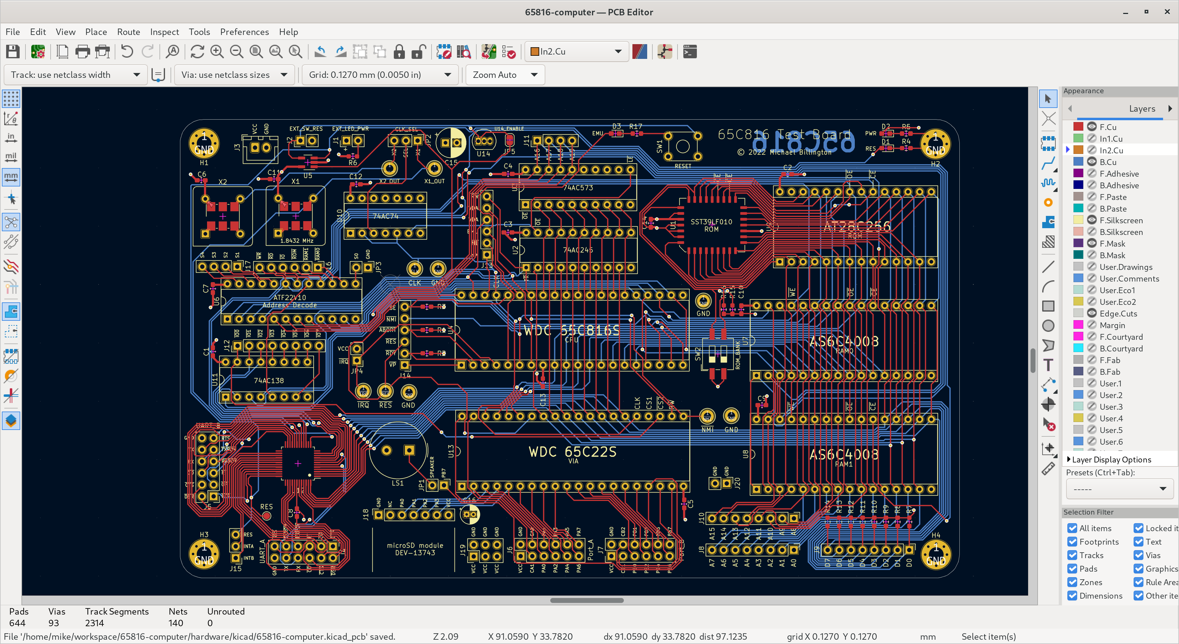
I put a lot of time into labeling different parts of the board to help with debug/assembly, and used the 3D view to check that it wasn’t too crowded.
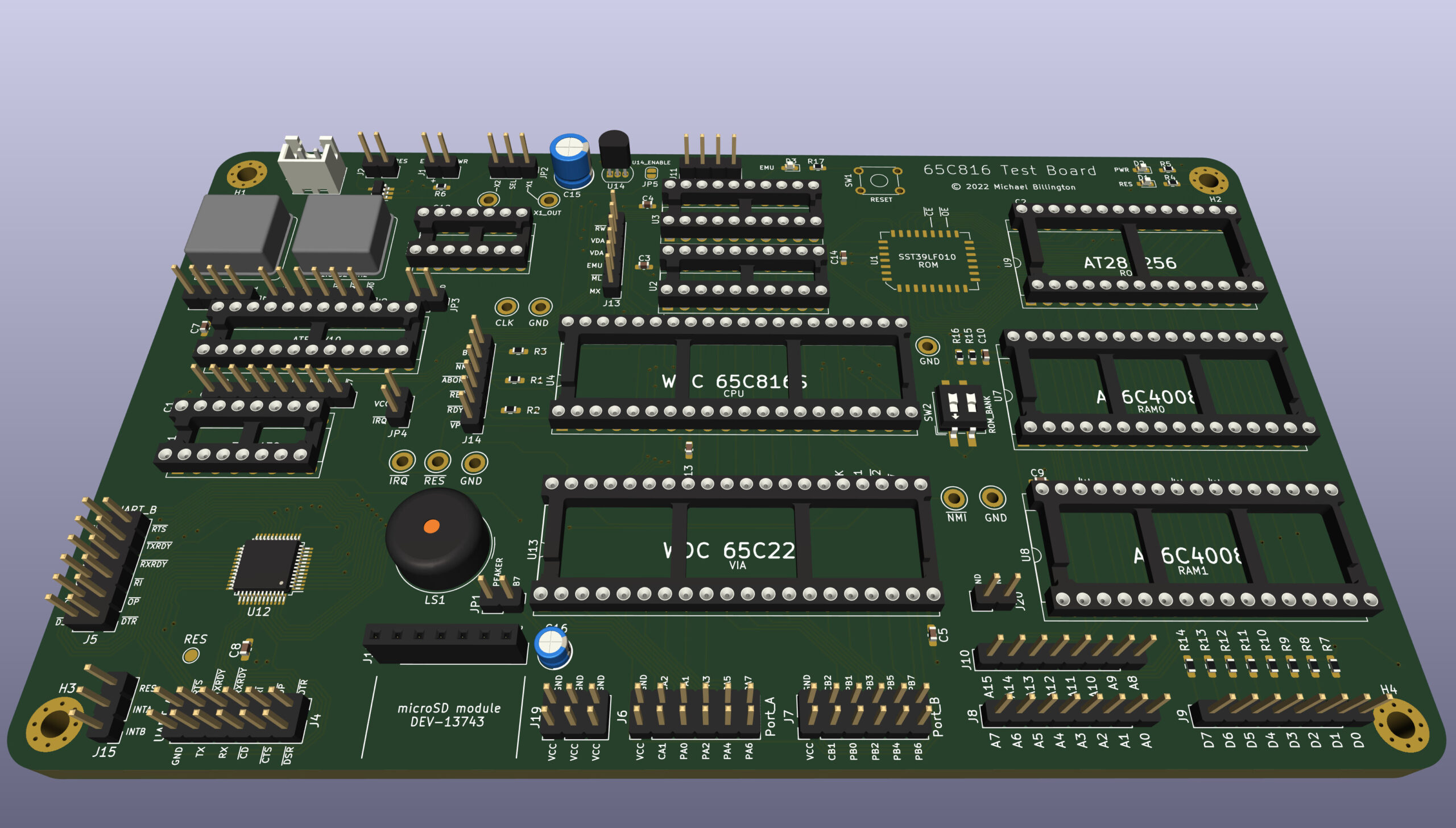
Before sending the files to a manufacturer, I printed it at 1:1 scale for a reality check.
Among other things, this confirmed that the ROM sockets had enough clearance from other components.
It also confirmed that either DIP-8 or QFN-packaged oscillators would fit.
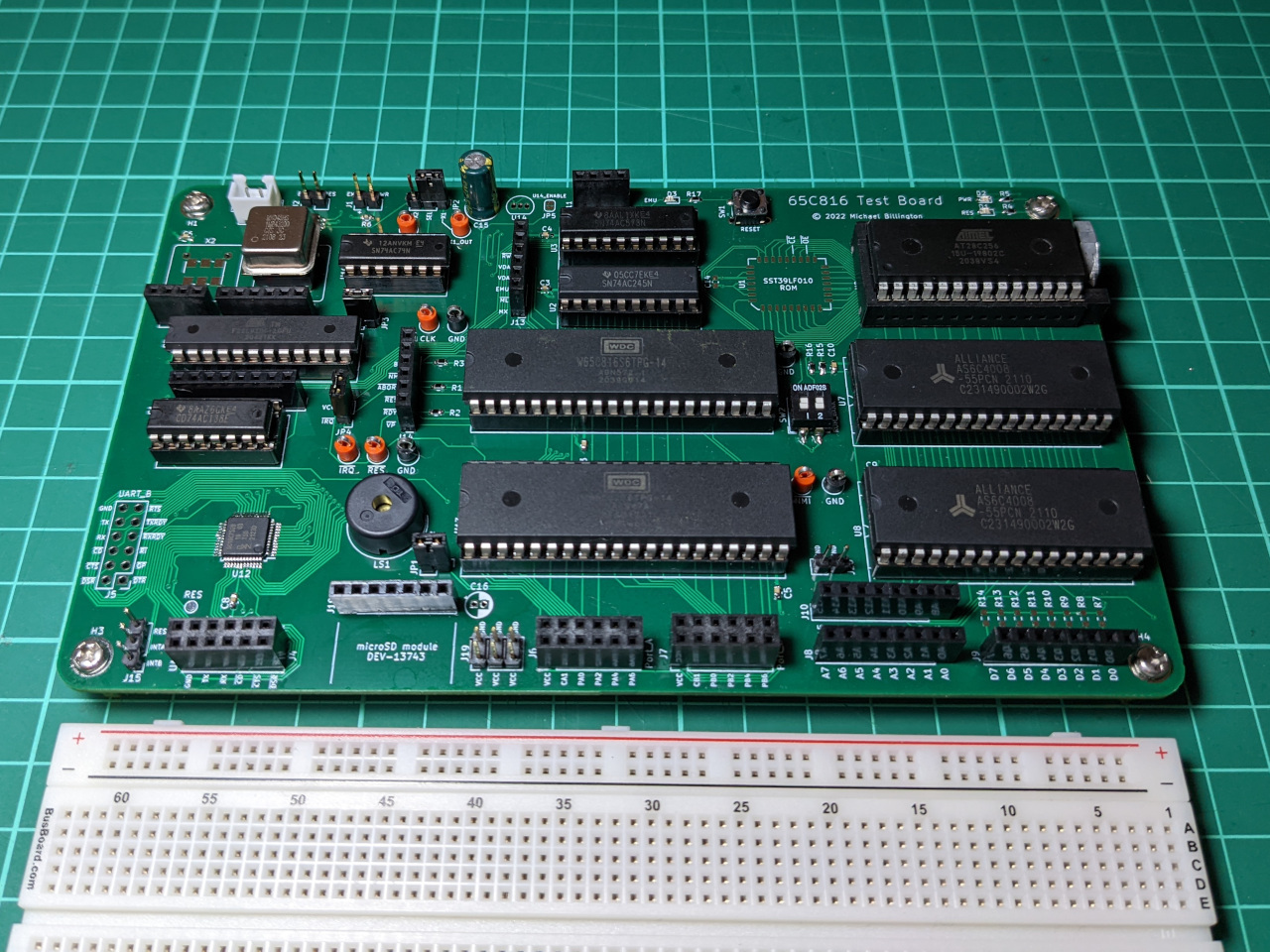
Assembly
I ordered the boards from a manufacturer which I’ve used before. They are large-ish, lead-free 4-layer boards, but I’m not optimising for cost. I’ve left a lot of options in the board, so I’m hoping to make use of several of these PCBs in different configurations, depending on which direction this project goes.
![]()
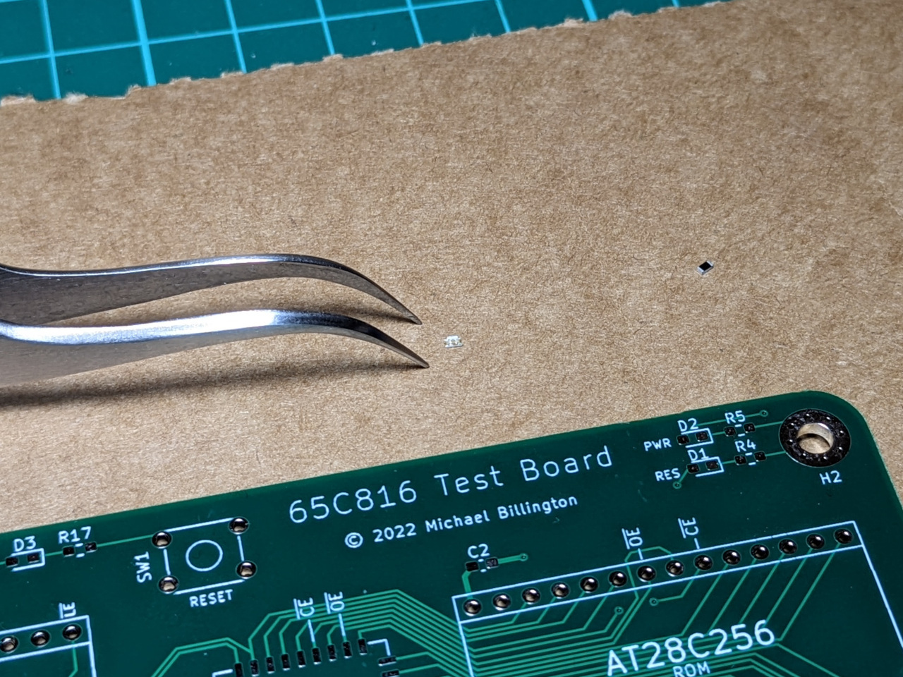
I assembled the board incrementally, starting with the power LED. Most of the passive components on this board are 0603 (imperial) size surface-mount parts, and I’ve used footprints with long pads for hand soldering.
The first problem I found was with the reset button - I had switched to using a footprint with the correct pin spacing, but had assigned the pins incorrectly, so I needed to cut/bend some legs and install it rotated 90 degrees.
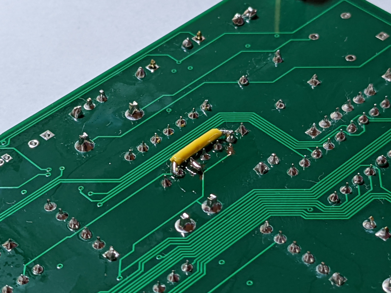
I next found a problem with the clock, where I had wired up the flip-flop incorrectly in the schematic - the /Q output should go to D. I could recover from this by cutting a trace and running a short wire. Of course the board is mirrored when flipped upside-down, so I cut the wrong trace first and needed to repair that too.
I added enough components to get the CPU to run NOP instructions from ROM, then built up to a running some test programs which I’ve blogged about here. The final mistake I discovered was a mix-up with some of the lines used for selecting I/O devices, which means that devices are not mapped to their intended addresses. I can work around this in software.
This is already an improvement over the breadboard prototype, because I can quickly swap the ROM chip without accidentally disconnecting anything.
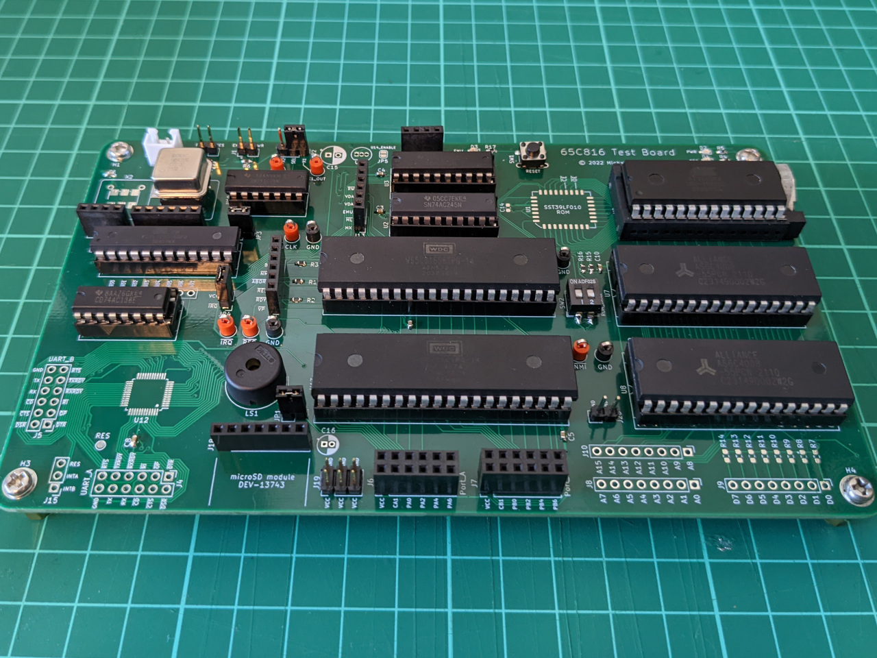
The board looked fairly complete at this point, and the only major component missing was the UART chip. This was the part which did not work reliably in my prototype, so I was prepared to do some debugging here. Note that I’ve got orange test points all over the board to connect important signals to an oscilloscope, with a few black test points for GND connections. All of the 74-series chips are in the 74AC logic family, and I sourced 74HC versions as well in case I needed to switch any to see the difference.
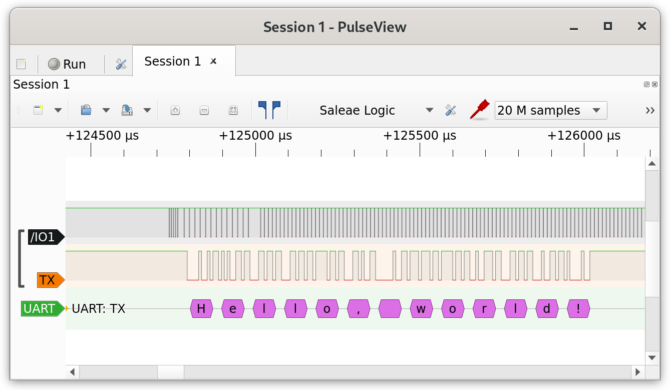
However, I was able to run more or less the same test program I used before, and it now works reliably. This is captured through a Cypress FX2-based logic analyser using Sigrok.
It’s great that this works, but I don’t know for sure why this was so unreliable on my previous prototype. Several possible causes were eliminated through this process, since I used a new UART chip and freshly programmed address decode PLD, and eliminated a possible timing issue. On a PCB, I’m also able to make better electrical connections, and add a ground plane, which is an immediate advantage over breadboards.
The design as it stands
Now that I am back to having a working prototype, I’ll take this chance to post some updated schematics.
Just a note of caution: this is snapshot of a work-in-progress learning project. I’m absolutely aware that there are errors in here, and that the layout is quite messy. Still, I hope that this is useful to anybody else who is attempting to use this relatively obscure CPU.
The design no longer fits on one page, so I’ve split it into 3 sheets.

CPU
The CPU sheet contains the circuitry for de-multiplexing the data bus and bank address byte. All power, reset, and clock components are in here as well, along with pin headers for the address & data bus, and all those test points.
There are a lot of “just in case” components as well, such as pull-up resistors on the data bus, which I have not fitted.

Memory
The memory section is quite straightforward. I’ve got a PLD generating chip-selects for ROM, RAM0, or RAM1, with some extra components to add some flexibility.

I/O
In case I/O is selected, there are three possible choices: the 65C22 VIA, or one of the two UART interfaces. Most of the other components on this sheet are optional footprints or external ports. Note that the clock going into the UART is mis-labelled on this sheet.

Next steps
I’m going to spend some time using this board as a development platform for low-level software which targets the 65C816 CPU. I’ll most likely also use the emulator which I put together a few weeks ago to speed up development, since I’ve been able to confirm that the code I’m writing works on real hardware.
The basic functionality is now a lot more stable than what I had before, so this test board will allow me to prototype some different hardware options once I’ve got some simple text-based programs up and running.
The hardware design, software and emulator for this computer can be found in the GitHub repository for this project. I’m updating the repository as I make progress with this project, and the version used for this blog post is here.