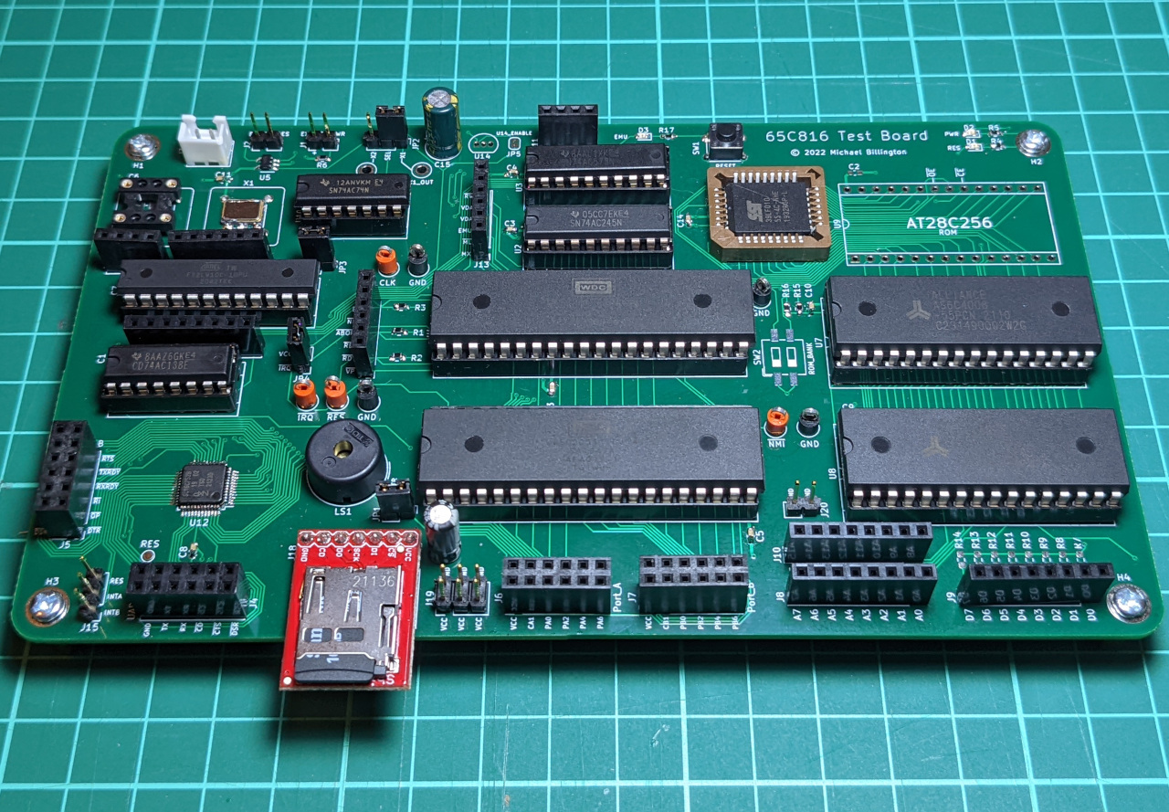
I recently spent some time re-building my 65C816 computer project to run at 3.3 volts, instead of 5 volts which it used previously. This blog post covers some of the things I needed to take into consideration for the change.
It involved making use of options which I added when I designed this test board, as well as re-visiting all of the mistakes in that design.
Re-cap: Why 3.3 V is useful
One of the goals of this project is to build a modern computer which uses a 65C816 CPU, using only in-production parts.
A lot of interesting retro chips run at 5 V, but it’s much easier to find modern components which run at 3.3 V. I can make use of these options without adding level-shifting if I can switch important buses and control signals to 3.3 V.
ROM
The ROM chip is the most visible change, because the chip has a different footprint. When assembling this board for 5 V use, I used an AT28C256 Parallel EEPROM, in a PDIP-28 ZIF socket. I couldn’t find 3.3 V drop-in replacement for this, so I added a footprint for a SST39LF010 flash chip, which has a similar-enough interface.
This was the first time I’ve soldered a surface-mount PLCC socket. I attempted to solder this with hot air, which was unsuccessful, so I instead cut the center of the socket out so that I could use a soldering iron. I then added a small square of 1000 GSM card (approx 1mm thick) as a spacer under the chip.
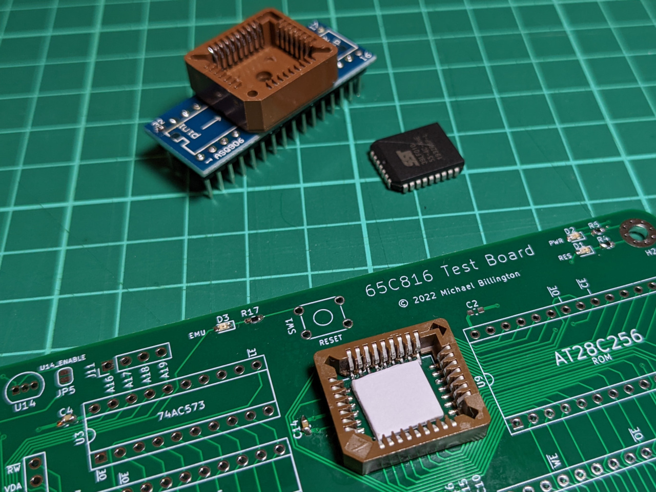
I also added a new make target to build the system ROM for this chip, which involves padding the file to a larger size, and invoking minipro with a different option so that it could write the file. I’m using a TL866II+ for programming, and adapter boards are available for programming PLCC-packaged chips.
$ make flashrom_sst39lf010
cp -f rom.bin rom_sst39lf010.bin
truncate -s 131072 rom_sst39lf010.bin
minipro -p "SST39LF010@PLCC32" -w rom_sst39lf010.bin
Found TL866II+ 04.2.126 (0x27e)
Warning: Firmware is newer than expected.
  Expected  04.2.123 (0x27b)
  Found     04.2.126 (0x27e)
Chip ID OK: 0xBFD5
Erasing... 0.40Sec OK
Writing Code...  8.38Sec  OK
Reading Code...  1.18Sec  OK
Verification OK
UART
The UART chip is an NXP SC16C752B, which is 3.3 V or 5 V compatible. I rescued one of these from an adapter board (previous experiment). This was my first time de-soldering a component with hot air gun. Hopefully it still works!
My FTDI-based USB/UART adapter has a configuration jumper which I adjusted to 3.3 V.
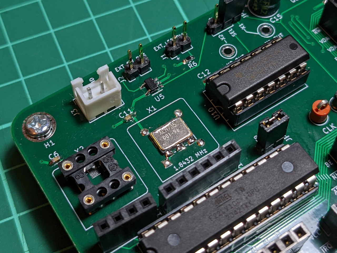
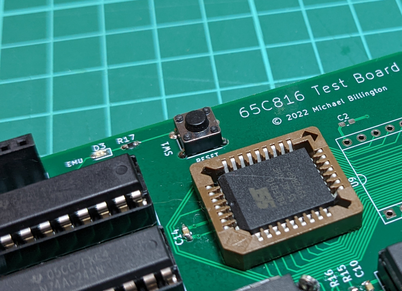
Clock, reset and address decode
I again used a MIC2775 supervisory IC for power-on reset, though the exact part was different. I previously used a MIC2275-46YM5 (4.6 V threshold), where the re-build used a MIC2275-31YM5 (3.1 V threshold).
I needed a 1.8432 MHz oscillator for the UART. The 3.3 V surface-mount part I substituted in had a different footprint, which I had prepared for.
I also prepared for this change by using an ATF22LV10 PLD for address decoding, which is both 3.3 V and 5 V compatible. The ATF22V10 which I used for earlier experiments works at 5 V only.
SD card
I installed the DEV-13743 SD card module more securely this time by soldering it in place and adding some double-sided tape as a spacer. This module is compatible with 3.3 V or 5 V.
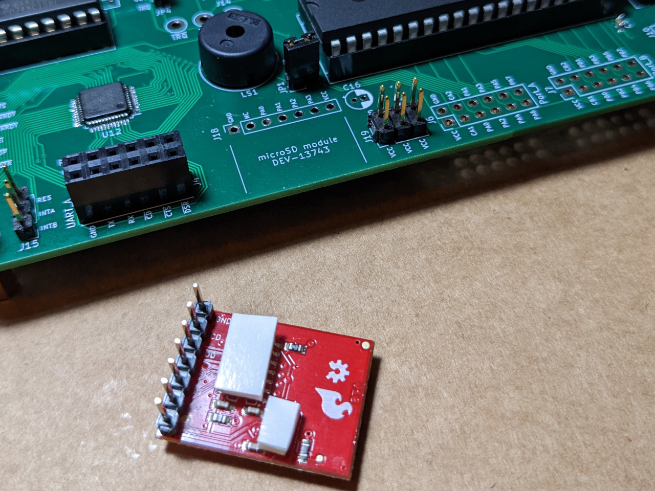
The level-shifting and voltage regulation on this module is now superfluous, so I could probably simplify things by adding an SD card slot and some resistors directly in a later revision.
Modifications
There are three errors in the board which I know about (all described in my earlier blog post). This is my second time fixing them, so I tried to make sure the modifications were neat and reliable this time.
Firstly, the flip-flop used as a clock divider is wired up incorrectly, so I cut a trace and run a wire under the board.
Second, the reset button pin assignments are incorrect. Simply rotating the button worked on the previous board, but it wasn’t fitted securely. This time I cut one of the legs and ran a short wire under the board, and the modification is barely noticeable.
Lastly, the address bus is wired incorrectly into the chip which selects I/O devices. I previously worked around this in software, but this time I cut two traces and ran two wires (the orange wires in the picture). I made an equivalent modification to the 5 V board, so that I could update the software and test it.
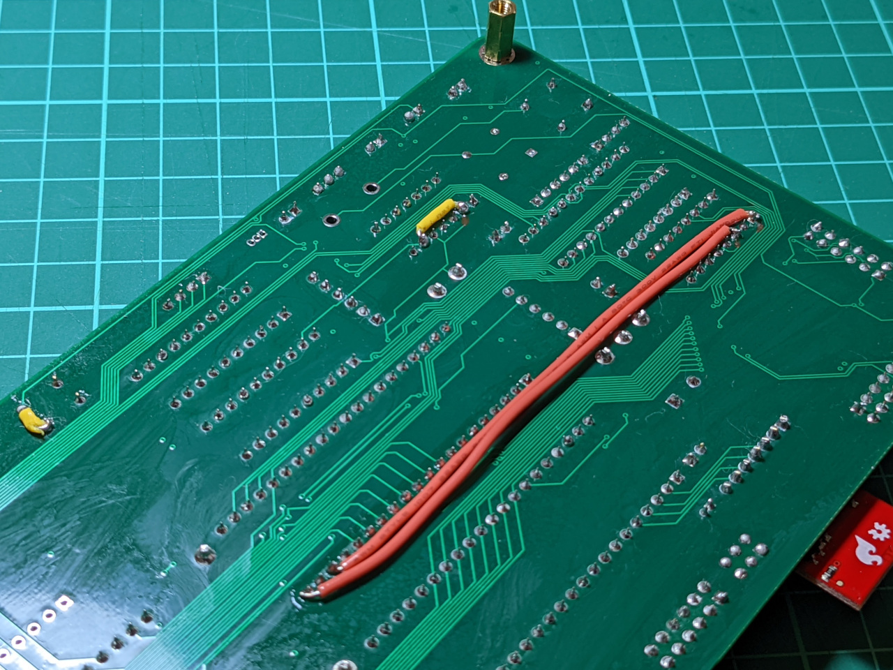
The wire I was using for these mods is far too thick and inflexible. I’ve added some 30 AWG silicon-insulated wire to my inventory for the next time I need to do this type of work, which should be more suitable.
Wrap-up
I transferred components from the old board, and attempted to boot it every time I made change. The power-on self test routine built in to the ROM showed that each new chip was being detected, and I soon had a working 65C816 test board again, now running at 3.3 V. I’m using my tiny linear power supply module to power it.
I can now interface to a variety of chips which only run at 3.3 V. This opens up some interesting possibilities for adding peripherals, which I hope to explore in future blog posts.
It will be more difficult to remove and re-program the ROM chip going forward though. This is hopefully not a problem, since can now run code from an SD card or serial connection as well (part 1, part 2).