A few weeks ago, I blogged about my setup for programming PLD’s from Linux, which are the simpler ancestors of modern FPGA’s.
The device I’m using is the ATF22V10, and programming it in involved running decades-old proprietary software called WinCUPL under WINE. I recently found an opportinity to test-run an open-source alternative, galette, and this blog post is a few notes about how it went.
Re-visiting my assumptions
The Atmel ATF22V10 is pin-compatible with the Lattice GAL22V10, which was discontinued over 10 years ago. There is a lot more information and software available for Lattice GAL’s, which I assume had the mind-share back when these devices were relevant.
There are some slight differences between the Atmel and Lattice devices. Some programming hardware works with one but not the other, and I had assumed that the fuse map (JED file) would be incompatible as well. This turned out to be incorrect.
A few statements online made me look at this again “You can also write Lattice GAL maps to the Atmel ATF16V8 and 22V10 parts” (Andrew B on retrobrewcomputers.org), and “The most suitable replacement for the GAL22V10 from Atmel is the ATF22V10C/CQ/CQZ. They are pin-to-pin and JEDEC fusemap compatible.” (GAL22V10 replacement on the Microchip knowledgebase).
The open source tool galette can create JED files for the Lattice GAL22V10, so I decided to try to write its output to an ATF22V10 to see for myself.
Detour: Installing a Rust toolchain
Galette is written in Rust, and available only as source code at the time of writing. The instructions for setting up Rust are online here.
apt install curl
curl --proto '=https' --tlsv1.2 -sSf https://sh.rustup.rs | sh
Then to compile any Rust project is the same process:
$ cargo build
Finding an example JED file
Next I tried running the tests, which did not pass
$ ./run_tests.sh
I found that this was simply the assembler version being different, plus a trailing number (maybe a checksum?).
diff -ru baseline/vcc.jed test_tmp/vcc.jed
--- baseline/vcc.jed    2021-08-19 20:16:20.526847059 +1000
+++ test_tmp/vcc.jed    2021-08-19 20:26:00.367537520 +1000
@@ -1,5 +1,5 @@

-GAL-Assembler:  Galette 0.2.0
+GAL-Assembler:  Galette 0.3.0
 Device:         GAL16V8

 *F0
@@ -25,4 +25,4 @@
 *L2193 0
 *C3c8f
 *
-924f
+9250
I then took one of the test outputs, and tried writing it to a device. As detailed in my earlier blog post, I’m using minipro, with a TL866II+ programmer, which could only program these devices after a firmware update.
$ minipro -p ATF22V10CQZ -w baseline/GAL22V10_combinatorial.jed
Found TL866II+ 04.2.126 (0x27e)
Warning: Firmware is newer than expected.
  Expected  04.2.123 (0x27b)
  Found     04.2.126 (0x27e)

VPP=12V
Warning! JED file doesn't match the selected device!

Declared fuse checksum: 0x87E2 Calculated: 0x87E2 ... OK
Declared file checksum: 0x12CF Calculated: 0x12D0 ... Mismatch!
JED file parsed OK

Use -P to skip write protect

Erasing... 0.33Sec OK
Writing jedec file...  5.04Sec  OK
Reading device...  0.41Sec  OK
Writing lock bit... 0.36Sec OK
With failed tests, checksum errors, firmware version mismatch and device ID mismatch, I was not expecting this to work.
Checking the source for this file, one of the lines is a simple AND expression.
O0 = I0 * I1
I wired up two inputs and one output (pins 2, 3 and 14), to confirm that it behaved as expected.
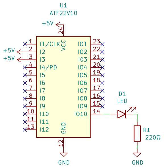
I used a multimeter to check that it was drawing a reasonably low current (about 7 mA). In previous experiments, these chips had made a lot of heat when programmed incorrectly.
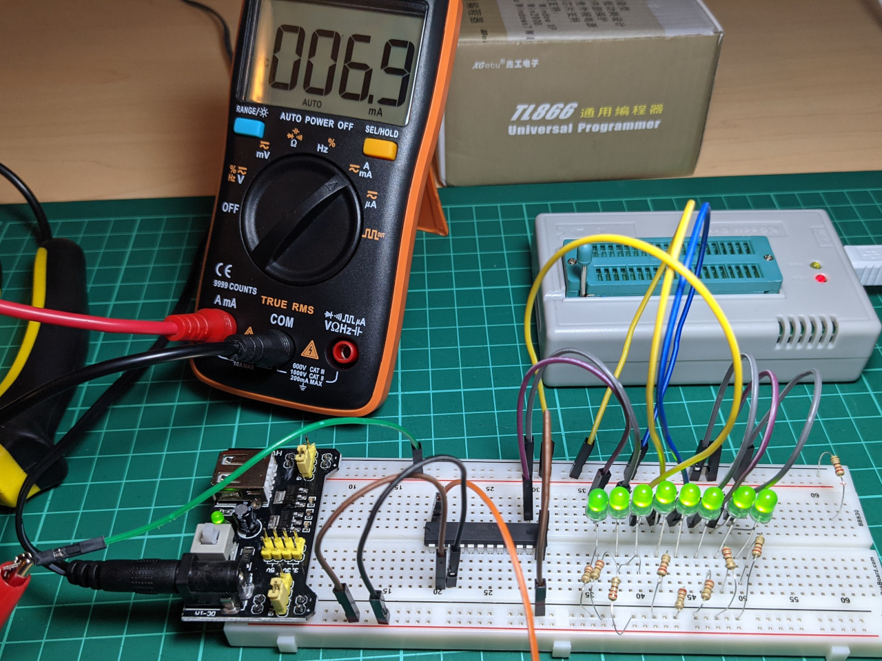
Everything worked, so this open-source replacement is looking good so far.
Update: I repeated the simple test of combinatorial logic in an ATF22LV10C running at 3.3v. At the time of writing, this ’low voltage’ variant is not listed as a supported chip in minipro, but can be programmed using the exact same procedure as an ATF22V10, and then operated at either 5V or 3.3V. The command I am using to program this chip is:
minipro -p ATF22V10CQZ -w baseline/GAL22V10_combinatorial.jed
Interfacing with a 6502 computer
I have some ideas for using programmable logic to extend my 6502-based computer, so I wanted to test tri-state output.
The previous test only used combinatorial output, where each pin is set high or low according to a logic function. For the ATF22V10, it should also possible to program an “output enable” function for each pin, in order to use tri-state logic. This would allow me to connect it to the 8-bit data bus on my home-built computer.
The best documentation for this was:
To test this, I programmed an ATF22V10 to output “42” (0010 1010) to the data bus when an output enable pin is low. In the source file, 0 is GND, and 1 is VCC.
Tri-state outputs are suffixed with .T, while outputs suffixed with .E are the “output enable” functions for that pin (the pin is high-impedance when false). I left one output in the combinatorial mode (always enabled), to verify that this is being controlled separately for each pin.
GAL22V10
Test1

NC    NC    I1    OE    NC    NC    NC    NC    NC    NC    NC   GND
NC    NC    O1    D7    D6    D5    D4    D3    D2    D1    D0   VCC

O1 = I1

D0.T = GND
D1.T = VCC
D2.T = GND
D3.T = VCC
D4.T = GND
D5.T = VCC
D6.T = GND
D7.T = GND

D0.E = /OE
D1.E = /OE
D2.E = /OE
D3.E = /OE
D4.E = /OE
D5.E = /OE
D6.E = /OE
D7.E = /OE

DESCRIPTION

Output 42 on the data bus when output is enabled.
I used my local build of Galette to generate a JED file, then wrote the JED file to the chip using the same process as before.
$ ./galette/target/debug/galette test1.pld
$ minipro -p ATF22V10CQZ -w test1.jed
I then built this test circuit, which connects one I/O select line from my computer to the PLD, plus the 8-bit data bus. The combinatorial output is connected to an LED for testing.
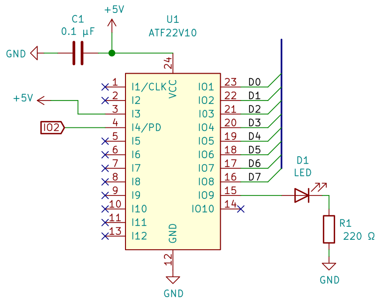
The IO2 input maps to address $8800 in my computer’s address decoding scheme. I have other blog posts about mapping new hardware devices into memory if you’re interested to know how that works.
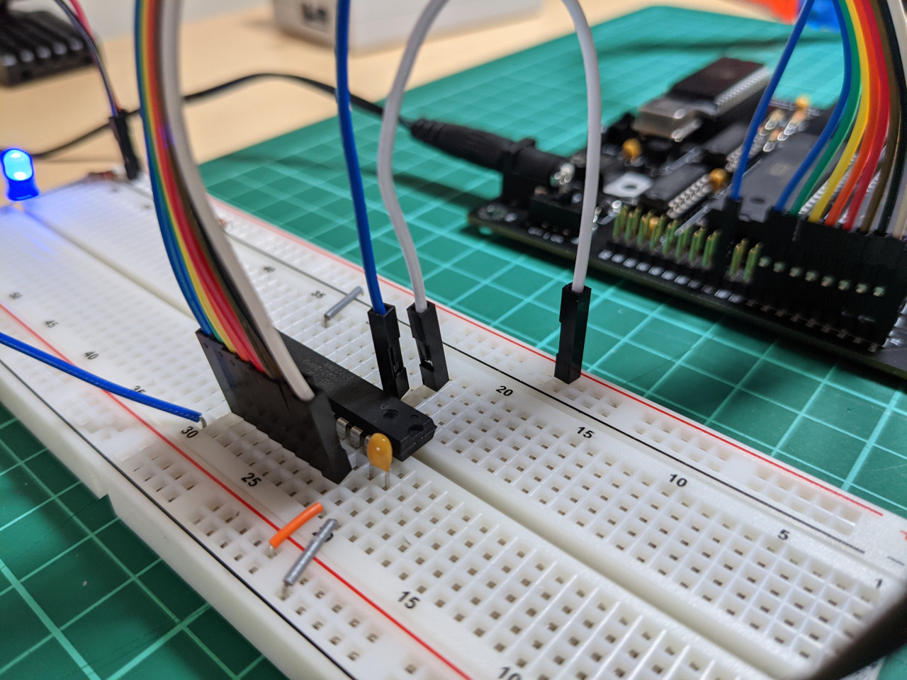
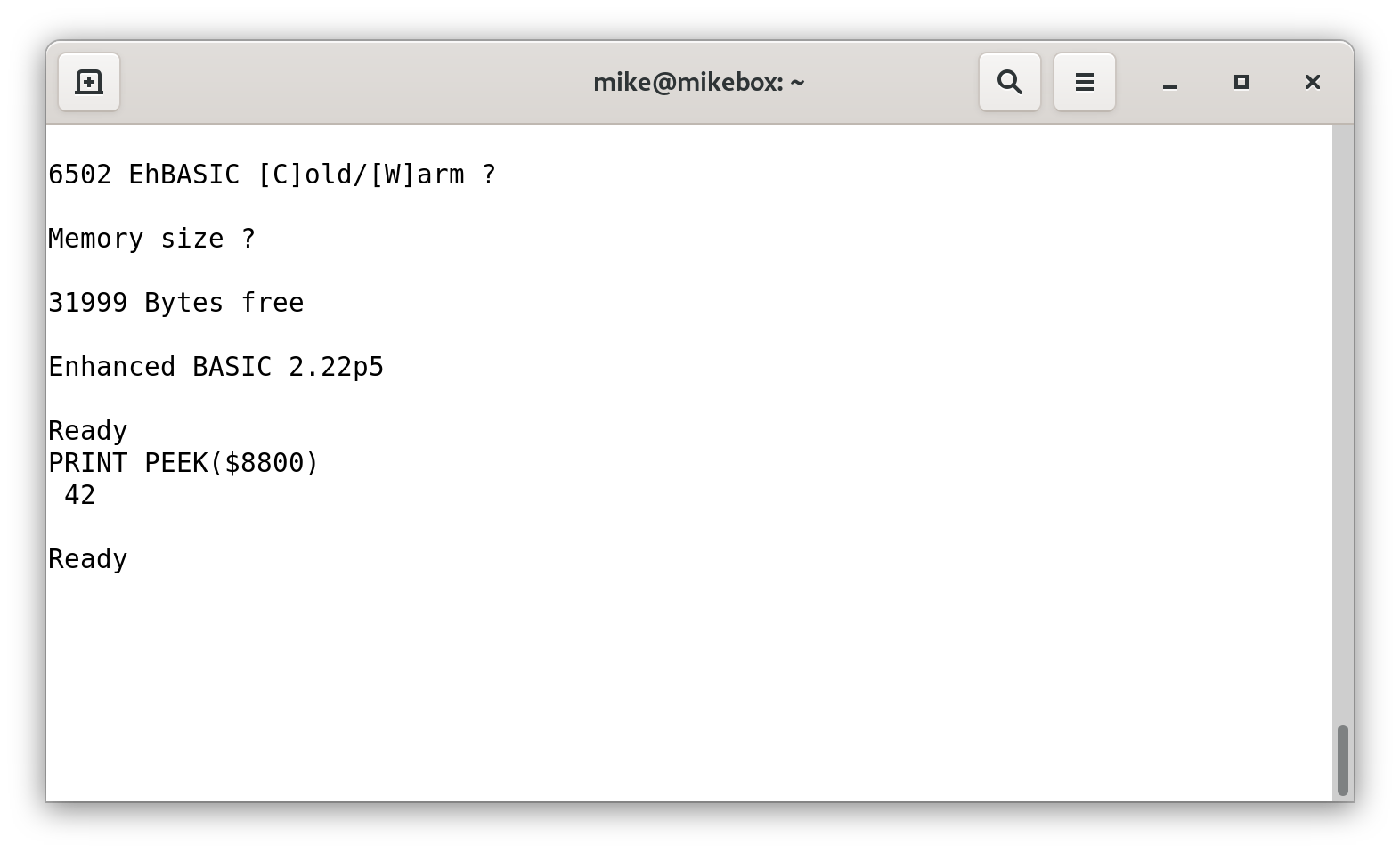
This computer boots to BASIC, and I was able to print “42” by reading this memory address via the PEEK command.
This also confirms that D0 is the least-significant bit in the data bus, which I was not sure of before.
Next steps
This has been an interesting discovery for me, and I’m planning to use Galette instead of WinCUPL for my electronics projects. PLD’s are relatively obscure, and it’s great to have an open-source tool for working with them. The only thing I will miss from WinCUPL it its test/simulation feature. I now need to program a chip and test it in a circuit, which is laborious, and I’m quickly using up the limited number of write cycles that these devices are rated for.
I created an “ATF22V10” symbol in KiCad to draw the schematics for this blog post, which is not particularly clear, since the pin names do not correspond with the ones defined in the .pld file. The next time I’m including one of these in a schematic, I’ll try creating a separate symbol for each programmed chip.
I’m planning to use an ATF22V10 PLD to build an interrupt controller for my computer, look out for a future blog post about that.