I am currently working on building a 65C816-based computer from scratch. I have some ideas for how I want to do this, but my first task is to put together a working prototype. I’ll be extending this in different ways to work towards the goals outlined in my last blog post.
This is about the simplest computer I can come up with which uses the 65C816 processor, but there is still quite a lot to go though.
Parts
All of the integrated circuits on this prototype are through-hole packages, suitable for use on a breadboard.
- WDC W65C816S CPU
- WDC W65C22S VIA I/O chip.
- Alliance AS6C4008-55PCN 512k x 8 55ns SRAM
- Atmel AT28C256 32k x 8 EEPROM
- Atmel ATF22LV10 PLD for address decoding
- 74AC04, 74AC245, 74AC573 for handling the multiplexed data bus and bank address bits
- 1.8432 MHz oscillator
- DS1813-5+ supervisory circuit
I also used the following equipment to program the chips, and view the result of the test program:
- TL-866II+ EEPROM programmer
- 8-channel Cypress FX2-based logic analyser
I’m working on Linux, and also use the following software tools:
- ca65 - for assembling code for the CPU
- minipro - for programming the EEPROM and PLD.
- galette - for assembling the logic definitions for the PLD.
- sigrok - for working with the logic analyser
Bank address latching
The 65C816 has a 24-bit address bus, and the top 8 bits are multiplexed onto the data bus. This is not a big problem, but it does mean that I need some extra glue logic compared to a plain 6502 system. A diagram in the 65C816 data sheet shows a suggestion for how to do this, and I’m starting with that implementation.
I used a 74AC04 to invert the clock, 74AC245 bus transceiver for the data bus, and a 74AC573 latch for the bank address (upper 8 bits of the address bus). This first page also shows the DS1813-5+ supervisory circuit on the reset line, which resets all of the components on power-up.

I’m aware that I should be generating a two-phase clock (there is some discussion about that here), though I can’t see any problems arising from the the delay on the inverted clock on this particular circuit.
Memory map and address decoding
The memory map for this computer is very simple. All of this will change, but I did need to start with something to get some code running.
Only the lower 19 bits of the address space are properly decoded, and mapped to one of three chips.
| Address | Maps to |
|---|---|
| 010000 - 07FFFF | RAM - 448 KiB |
| 00E000 - 00FFFF | ROM - 8 KiB |
| 00C000 - 00DFFF | I/O - 8 KiB |
| 000000 - 00BFFF | RAM - 48 KiB |
I used a programmable logic device (PLD) to implement this. It’s easy enough to do this with discrete gates, but a PLD will make it much easier to keep chip count and propagation delays under control as I add more features. I’ve written about programming PLD’s in previous blog posts (here, here and here), and I plan to use them to implement several features.
The particular part I am programming here is an ATF22LV10. These are still produced the time of writing, and operate at either 3.3 volts or 5 volts, which is useful for this project. They can be also programmed with the common TL-866II+ chip programmer, which I also use for programming EEPROMs.
The definitions for decoding this are below. I called this file address_decode.pld.
GAL22V10
AddrDecode

Clock  RW     NC     NC     A19    A18    A17    A16    A15    A14    A13    GND
NC     /RAMCS /ROMCS /IOCS  /RD    /WR    NC     NC     NC     NC     NC     VCC

; ROM is the top 8 KiB of bank 0.
; prefix is 0000 111xxxxx xxxxxxxx
ROMCS = /A19*/A18*/A17*/A16*A15*A14*A13

; IO addresses are mapped below ROM in bank 0.
; prefix is 0000 110xxxxx xxxxxxxx
IOCS = /A19*/A18*/A17*/A16*A15*A14*/A13

; RAM is selected for any address does *not* match 0000 11xxxxxx xxxxxxxx
RAMCS = A19 + A18 + A17 + A16 + /A15 + /A14

; Qualify writes with clock
RD = RW
WR = Clock*/RW

DESCRIPTION

Address decode logic for 65C816 computer.

ROM is top 8K of bank 0, I/O is 8k below that, everything else is RAM.
I assembled this with galette:
galette address_decode.pld
This generates a .jed file, which can be used to program the chip. The ATF22LV10 is not on the compatibility list for my programmer, but it works just fine if I identify it as an ATF22V10CQZ.
minipro -p ATF22V10CQZ -w address_decode.jed

Firmware and testing
I came up with a simple test program which would require working ROM, RAM, and I/O. The CPU boots to 6502 emulation mode, and this test program does not access memory outside bank 0.
I created a linker configuration file which mostly reflects the system’s memory map, and called it system.cfg.
MEMORY {
    ZP:     start = $00,    size = $0100, type = rw, file = "";
    RAM:    start = $0100,  size = $7e00, type = rw, file = "";
    PRG:    start = $e000,  size = $2000, type = ro, file = %O, fill = yes, fillval = $00;
}

SEGMENTS {
    ZEROPAGE: load = ZP,  type = zp;
    BSS:      load = RAM, type = bss;
    CODE:     load = PRG, type = ro,  start = $e000;
    VECTORS:  load = PRG, type = ro,  start = $fffa;
}
I then wrote this test program, main.s. The program runs from ROM, and writes a hard-coded value to one of the output ports. It then stores a 0 in RAM, then increments it and stores that to an output port in an infinite loop, which will show a counting pattern if RAM can be read and written.
PORTB = $c000
DDRB = $c002

SOME_ADDRESS_IN_RAM = $beef

.segment "CODE"

; Write 42 to VIA port B
reset:
  lda #%11111111 ; Set all pins to output
  sta DDRB

  lda #42
  sta PORTB

; Start at 0, and increment a value in RAM
  lda #00
  sta SOME_ADDRESS_IN_RAM

loop:
  inc SOME_ADDRESS_IN_RAM
  lda SOME_ADDRESS_IN_RAM
  sta PORTB			; Output the value
  jmp loop

nmi:
  rti

irq:
  rti

.segment "VECTORS"
.word nmi
.word reset
.word irq
I assembled this with ca65, then linked it with ld65. As far as the assembler knows, it is generating code for a 6502 CPU, not a 65C816. I am not using any advanced features, so this should be fine for this test.
ca65 main.s
ld65 -o rom.bin -C system.cfg main.o
This outputs an 8 KiB binary file, which is the amount of ROM space mapped in the computer’s memory. The chip is actually 32 KiB though, so I filled the rest with zeroes.
truncate -s 32768 rom.bin
I then wrote the program to the EEPROM using minipro.
minipro -p AT28C256 -w rom.bin
I ran this program, with a logic analyser connected to port B of the 65C22 VIA. The capture below shows the initial hard-coded number, followed by the counting pattern, which indicates that everything is working as expected.

Wrap-up
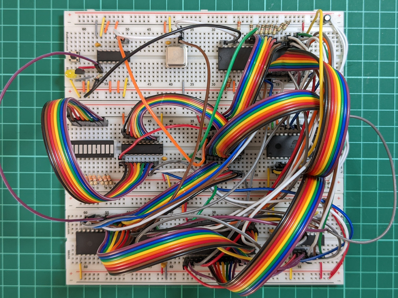
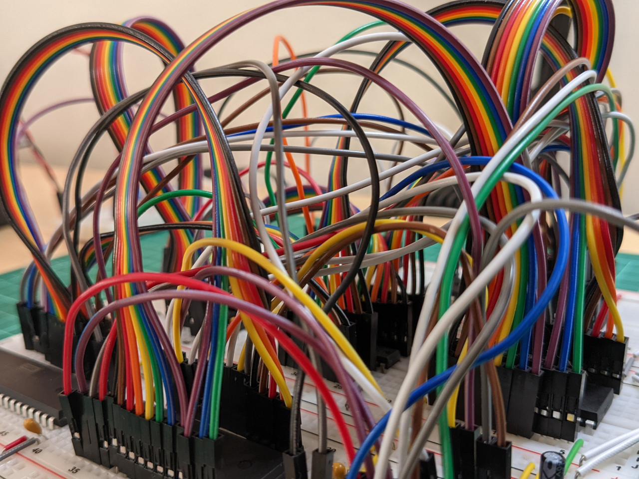
I’m starting simple here, so that I have a working base system to modify. Everything seems to be working fine on breadboards, so I’ll proceed with that for now. I may still need to re-build everything with shorter wires, since this is getting quite difficult to work with.
It is also worth noting that most of the components here should run at 3.3 volts, which is where this project is eventually headed. Only the clock, reset IC and EEPROM would need to be substituted at the moment.
This blog post is only a snapshot of the project. You can check the current status on GitHub here.